Tuesday, September 2, 2008

5 band graphic equalizer using a single IC/chip


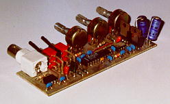
This circuit uses a single chip, IC BA3812L for realizing a 5 band graphic equalizer for use in hi-fi audio systems.The BA3812L is a five-point graphic equalizer that has all the required functions integrated onto one IC. The IC is comprised of the five tone control circuits and input and output buffer amplifiers. The BA3812L features low distortion, low noise, and wide dynamic range, and is an ideal choice for Hi-Fi stereo applica-tions. It also has a wide operating voltage range (3.5V to 16V), which means that it can be adapted for use with most types of stereo equipment.
The five center frequencies are independently set using external capacitors, and as the output stage buffer amplifier and tone control section are independent circuits, fine control over a part of the frequency bandwidth is possible, By using two BA3812Ls, it is possible to construct a 10-point graphic equalizer. The amount of boost and cut can be set by external components.
The recommended power supply is 8V, but the circuit should work for a supply of 9V also. The maximum voltage limit is 16V.
The circuit given in the diagram operates around the five frequency bands:
100Hz
300Hz
1kHz
3kHz
10kHz

Programmable Digital Code Lock


A programmable code lock can be used for numerous applications in which access to an article/gadget is to be restricted to a limited number of persons. Here is yet another circuit of a code lock employing mainly the CMOS ICs and thumbwheel switches (TWS) besides a few other components. It is rugged and capable of operation on voltages ranging between 6 and 15 volts. The supply current drain of CMOS ICs being quite low, the circuit may be operated even on battery.The circuit uses two types of thumbwheel switches. switch numbers TWS1 through TWS8 are decimal-to-BCD converter type while switch numbers TWS9 through TWS16 are 10-input multiplexer type in which only one of the ten inputs may be connected to the output (pole). One thumbwheel switch of each of the two types is used in combination with IC CD4028B (BCD to decimal decoder) to provide one digital output.Eight such identical combinations of thumbwheel switches and IC CD4028 are used. The eight digital outputs obtained from these combinations are connected to the input of 8-input NAND gate CD4068.For getting a logic high output, say at pole-1, it is essential that decimal numbers selected by switch pair TWS1 and TWS9 are identical, as only then the logic high output available at the Specific output pin of IC1 will get transferred to pole-1. Accordingly, when the thumbwheel pair of switches in each combination is individually matched, the outputs at pole-1 to pole-8 will be logic high.This will cause output of 8-input NAND gate IC CD4068b to change over from logic high to logic low, thereby providing a high-to-low going clock pulse at clock input pin of 7-stage counter CD4024B, which is used here as a flip-flop (only Q0 output is used here).The output (Q0) of the flip-flop is connected to a relay driver circuit consisting of transistors T1 and T2. The relay will operate when Q0 output of flip-flop goes low. As a result transistor T1 cuts off and T2 gets forward biased to operate the relay.Switch S1 is provided to enable switching off (locking) and switching on (unlocking) of the relay as desired, once the correct code has been set.With the code set correctly, the NAND gate output will stay low and flip-flop can be toggled any number of times, making it possible to switch on or switch off the relay, as desired. Suppose we are using the system for switching-on of a deck for which the power supply is routed via the contacts of the relay. The authorised person would select correct code which would cause the supply to become available to the deck. After use he will operate switch S1 and then shuffle the thumbwheel switches TWS1 through TWS8 such that none of the switches produces a correct code. Once the code does not match, pressing of switch S1 has no effect on the output of the flip-flop.Switches TWS9 through TWS16 are concealed after setting the desired code. In place of thumbwheel switches TWS1 through TWS8 DIP switches can also be used

Super simple stepper motor controller


The circuit shown above can be used to control a unipolar stepper motor which has FOUR coils (I've swiped it off an old fax machine). The above circuit can be for a motor current of up to about 500mA per winding with suitable heat sinks for the SL100. For higher currents power transistors like 2N3055 can be used as darlington pair along with SL100. The diodes are used to protect the transistor from transients.

Sawtooth wave generator


Sawtooth wave generators using opamp are very common. But the disadvantage is that it requires a bipolar power supply.
A sawtooth wave generator can be built using a simple 555 timer IC and a transistor as shown in the circuit diagram.
The working of the circuit can be explained as follows:The part of the circuit consisting of the capacitor C, transistor,zener diode and the resistors form a constant current source to charge the capacitor. Initially assume the capacitor is fully discharged. The voltage across it is zero and hence the internal comparators inside the 555 connected to pin 2 causes the 555's output to go high and the internal transistor of 555 shorting the capacitor C to ground opens and the capacitor starts charging to the supply voltage. As it charges, when its voltage increases above 2/3rd the supply voltage, the 555's output goes low, and shorts the C to ground, thus discharging it. Again the 555's output goes high when the voltage across C decreases below 1/3rd supply. Hence the capacitor charges and discharges between 2/3rd and 1/3rd supply.
Note that the output is taken across the capacitor. The 1N4001 diode makes the voltage across the capacitor go to ground level (almost).
The frequency of the circuit is given by:
f = (Vcc-2.7)/(R*C*Vpp)

Zener Diode Tester


Here is a handy zener diode tester which tests zener diodes with breakdown voltages extending up to 120 volts. The main advantage of this circuit is that it works with a voltage as low as 6V DC and consumes less than 8 mA current. The circuit can be fitted in a 9V battery box. Two-third of the box may be used for four 1.5V batteries and the remaining one-third is sufficient for accommodating this circuit. In this circuit a commonly available transformer with 230V AC primary to 9-0-9V, 500mA secondary is used in reverse to achieve higher AC voltage across 230V AC terminals. Transistor T1 (BC547) is configured as an oscillator and driver to obtain required AC voltage across transformer’s 230V AC terminals. This AC voltage is converted to DC by diode D1 and filter capacitor C2 and is used to test the zener diodes. R3 is used as a seri- es current limiting resistor. After assembling the circuit, check DC voltage across points A and B without connecting any zener diode. Now switch on S1. The DC voltage across A-B should vary from 10V to 120V by adjusting potmeter VR1 (10k). If every thing is all right, the circuit is ready for use. For testing a zener diode of unknown value, connect it across points A and B with cathode towards A. Adjust potmeter VR1 so as to obtain the maximum DC voltage across A and B. Note down this zener value corresponding to DC voltage reading on the digital multimeter. When testing zener diode of value less than 3.3V, the meter shows less voltage instead of the actual zener value. However, correct reading is obtained for zener diodes of value above 5.8V with a tolerance of ± 10per cent. In case zener diode shorts, the multimeter shows 0 volts

Dome light dimmer for Cars -designed by Naveen P N


This unique circuit makes your dome light look cool. Usually when the car door is closed, the dome light just goes OFF. With this circuit, you can have our dome light fade slowly in brightness and finally go OFF. This slow dimming of the light gives a very good feeling at night. It looks very romantic! The circuit can be explained as follows: When the car door is open, the push to off switch of the door is ON and hence it charges the 22uF capacitor fully. The opamp is acting as a voltage follower and its output is same as the voltage across the capacitor, which is 12V when the capacitor is fully charged. Due to a high voltage at the output of the IC, the transistor saturates, turning ON the bulb to full brightness.
Now when the door is closed, the door switch is pushed in and hence the switch goes OFF. When the switch is OFF, the capacitor starts discharging slowly through VR1 and the 10K resistor and the voltage across it decreases slowly. Hence at the output of IC 741 also the voltage decreases gradually, hence decreasing the base current to the transistor. This produces a slowly decreasing current through the bulb and the bulb fades out and finally when the capacitor is fully discharged, the bulb goes OFF.After building the circuit, with the push-to-off switch in ON position (not pushed in) i.e. the car door open, adjust the preset VR2 to the required initial brightness of the bulb. Then push the switch in to turn it OFF(or close the door) and adjust VR1 for the time to bring the bulb from full brightness to OFF.I would suggest you set VR1 and VR2 to their maximum values.

Car anti theft wireless alarm.


This FM radio-controlled anti- theft alarm can be used with any vehicle having 6- to 12-volt DC supply system. The mini VHF, FM transmitter is fitted in the vehicle at night when it is parked in the car porch or car park. The receiver unit with CXA1019, a single IC-based FM radio module, which is freely available in the market at reasonable rate, is kept inside. Receiver is tuned to the transmitter's frequency. When the transmitter is on and the signals are being received by FM radio receiver, no hissing noise is available at the output of receiver. Thus transistor T2 (BC548) does not conduct. This results in the relay driver transistor T3 getting its forward base bias via 10k resistor R5 and the relay gets energised. When an intruder tries to drive the car and takes it a few metres away from the car porch, the radio link between the car (transmitter) and alarm (receiver) is broken. As a result FM radio module gene-rates hissing noise. Hissing AC signals are coupled to relay switching circ- uit via audio transformer. These AC signals are rectified and filtered by diode D1 and capacitor C8, and the resulting positive DC voltage provides a forward bias to transistor T2. Thus transistor T2 conducts, and it pulls the base of relay driver transistor T3 to ground level. The relay thus gets de-activated and the alarm connected via N/C contacts of relay is switched on. If, by chance, the intruder finds out about the wireless alarm and disconnects the transmitter from battery, still remote alarm remains activated because in the absence of signal, the receiver continues to produce hissing noise at its output. So the burglar alarm is fool-proof and highly reliable.

Flashy Christmas Lights


This simple and inexpensive circuit built around a popular CMOS hex inverter IC CD4069UB offers four sequential switching outputs that may be used to control 200 LEDs (50 LEDs per channel), driven directly from mains supply. Input supply of 230V AC is rectified by the bridge rectifiers D1 to D4. After fullwave rectification, the average output voltage of about 6 volts is obtained across the filter comprising capacitor C1 and resistor R5. This supply energises IC CD4069UB.All gates (N1-N6) of the inverter have been utilised here. Gates N1 to N4 have been used to control four high voltage transistors T1 to T4 (2N3440 or 2N3439) which in turn drive four channels of 50 LEDs each through current limiting resistors of 10-kilo-o Base drive of transistors can be adjusted with the help of 10-kilo-ohm pots provided in their paths. Remaining two gates (N5 and N6) form a low frequency oscillator. The frequency of this oscillator can be changed through pot VR1. When pot VR1 is adjusted To get the best results, a low leakage, good quality capacitor must be used for the timing capacitor C2

TV remote control Blocker -designed by Naveen P N


Just point this small device at the TV and the remote gets jammed . The circuit is self explanatory . 555 is wired as an astable multivibrator for a frequency of nearly 38 kHz. This is the frequency at which most of the modern TVs receive the IR beam . The transistor acts as a current source supplying roughly 25mA to the infra red LEDs. To increase the range of the circuit simply decrease the value of the 180 ohm resistor to not less than 100 ohm.
It is required to adjust the 10K potentiometer while pointing the device at your TV to block the IR rays from the remote. This can be done by trial and error until the remote no longer responds

JAM(Just A Minute) Circuit


This jam circuit can be used in quiz contests wherein any par- ticipant who presses his button (switch) before the other contestants, gets the first chance to answer a question. The circuit given here permits up to eight contestants with each one allotted a distinct number (1 to 8). The display will show the number of the contestant pressing his button before the others. Simultaneously, a buzzer will also sound. Both, the display as well as the buzzer have to be reset manually using a common reset switch. Initially, when reset switch S9 is momentarily pressed and released, all outputs of 74LS373 (IC1) transparent latch go ‘high’ since all the input data lines are returned to Vcc via resistors R1 through R8. All eight outputs of IC1 are connected to inputs of priority encoder 74LS147 (IC2) as well as 8-input NAND gate 74LS30 (IC3). The output of IC3 thus becomes logic 0 which, after inversion by NAND gate N2, is applied to latch-enable pin 11 of IC1. With all input pins of IC2 being logic 1, its BCD output is 0000, which is applied to 7-segment decoder/driver 74LS47 (IC6) after inversion by hex inverter gates inside 74LS04 (IC5). Thus, on reset the display shows 0. When any one of the push-to-on switches—S1 through S8—is pressed, the corresponding output line of IC1 is latched at logic 0 level and the display indicates the number associated with the specific switch. At the same time, output pin 8 of IC3 becomes high, which causes outputs of both gates N1 and N2 to go to logic 0 state. Logic 0 output of gate N2 inhibits IC1, and thus pressing of any other switch S1 through S8 has no effect. Thus, the contestant who presses his switch first, jams the display to show only his number. In the unlikely event of simultaneous pressing (within few nano-seconds difference) of more than one switch, the higher priority number (switch no.) will be displayed. Simultaneously, the logic 0 output of gate N1 drives the buzzer via pnp transistor BC158 (T1). The buzzer as well the display can be reset (to show 0) by momentary pressing of reset switch S9 so that next round may start. Lab Note: The original circuit sent by the author has been modified as it did not jam the display, and a higher number switch (higher priority), even when pressed later, was able to change the displayed number.

Simple Analog to Digital Converter


Normally analogue-to-digital con-verter (ADC) needs interfacing through a microprocessor to convert analogue data into digital format. This requires hardware and necessary software, resulting in increased complexity and hence the total cost.The circuit of A-to-D converter shown here is configured around ADC 0808, avoiding the use of a microprocessor. The ADC 0808 is an 8-bit A-to-D converter, having data lines D0-D7. It works on the principle of successive approximation. It has a total of eight analogue input channels, out of which any one can be selected using address lines A, B and C. Here, in this case, input channel IN0 is selected by grounding A, B and C address lines.Usually the control signals EOC (end of conversion), SC (start conversion), ALE (address latch enable) and OE (output enable) are interfaced by means of a microprocessor. However, the circuit shown here is built to operate in its continuous mode without using any microprocessor. Therefore the input control signals ALE and OE, being active-high, are tied to Vcc (+5 volts). The input control signal SC, being active-low, initiates start of conversion at falling edge of the pulse, whereas the output signal EOC becomes high after completion of digitisation. This EOC output is coupled to SC input, where falling edge of EOC output acts as SC input to direct the ADC to start the conversion.As the conversion starts, EOC signal goes high. At next clock pulse EOC output again goes low, and hence SC is enabled to start the next conversion. Thus, it provides continuous 8-bit digital output corresponding to instantaneous value of analogue input. The maximum level of analogue input voltage should be appropriately scaled down below positive reference (+5V) level.The ADC 0808 IC requires clock signal of typically 550 kHz, which can be easily derived from an astable multivibrator constructed using 7404 inverter gates. In order to visualise the digital output, the row of eight LEDs (LED1 through LED8) have been used, wherein each LED is connected to respective data lines D0 through D7. Since ADC works in the continuous mode, it displays digital output as soon as analogue input is applied. The decimal equivalent digital output value D for a given analogue input voltage Vin can be calculated from the relationship

WELCOME to APR Welding Academy


A.P.R. Welding Academy is registered as a private career college under the Private Career Colleges Act, 2005. We are dedicated to producing quality welders who not only meet industry standards, but have the welding skills necessary to become a skilled tradesperson.

Monday, September 1, 2008

Introduction to motherboards


The primary component of a computer is the motherboard (sometimes called the "mainboard"). The motherboard is the hub which is used to connect all of the computer's essential components.

PIC microcontroller


PIC is a family of Harvard architecture microcontrollers made by Microchip Technology, derived from the PIC1640[1] originally developed by General Instrument's Microelectronics Division. The name PIC initially referred to "Programmable Interface Controller"[2], but shortly thereafter was renamed "Programmable Intelligent Computer".[3]
PICs are popular with developers and hobbyists alike due to their low cost, wide availability, large user base, extensive collection of application notes, availability of low cost or free development tools, and serial programming (and re-programming with flash memory) capability

Microcontroller Design Final Projects


Bruce writes "This site contains 45 new microcontroller-based projects from this semester, plus 150 older projects. Projects include a turbidty meter, video games, and an electronic flower. All projects are designed and constructed by students during the last month of classes in the spring semester". Great stuff! Link.
make_magazine:http://blog.makezine.com/archive/2005/05/microcontroller.html

DC Motor-Driver H-Bridge Circuit


Physical motion of some form helps differentiate a robot from a computer. It would be nice if a motor could be attached directly to a chip that controlled the movement. But, most chips can't pass enough current or voltage to spin a motor. Also, motors tend to be electrically noisy (spikes) and can slam power back into the control lines when the motor direction or speed is changed.Specialized circuits (motor drivers) have been developed to supply motors with power and to isolate the other ICs from electrical problems. These circuits can be designed such that they can be completely separate boards, reusable from project to project.A very popular circuit for driving DC motors (ordinary or gearhead) is called an H-bridge. It's called that because it looks like the capital letter 'H' on classic schematics. The great ability of an H-bridge circuit is that the motor can be driven forward or backward at any speed, optionally using a completely independent power source.An H-bridge design can be really simple for prototyping or really extravagant for added protection and isolation. An H-bridge can be implemented with various kinds of components (common bipolar transistors, FET transistors, MOSFET transistors, power MOSFETs, or even chips).

Sunday, August 31, 2008

What is GPS?


The Global Positioning System (GPS) is a satellite-based navigation system made up of a network of 24 satellites placed into orbit by the U.S. Department of Defense. GPS was originally intended for military applications, but in the 1980s, the government made the system available for civilian use. GPS works in any weather conditions, anywhere in the world, 24 hours a day. There are no subscription fees or setup charges to use GPS.

Antenna (radio)


An antenna is a transducer designed to transmit or receive electromagnetic waves. In other words, antennas convert electromagnetic waves into electrical currents and vice versa. Antennas are used in systems such as radio and television broadcasting, point-to-point radio communication, wireless LAN, radar, and space exploration. Antennas usually work in air or outer space, but can also be operated under water or even through soil and rock at certain frequencies for short distances.
Physically, an antenna is an arrangement of conductors that generate a radiating electromagnetic field in response to an applied alternating voltage and the associated alternating electric current, or can be placed in an electromagnetic field so that the field will induce an alternating current in the antenna and a voltage between its terminals. Some antenna devices (parabolic antenna, Horn Antenna) just adapt the free space to another type of antenna.
Thomas Edison used antennas by 1885. Edison patented his system in U.S. Patent 465,971 . Antennas were also used in 1888 by Heinrich Hertz (1857-1894) to prove the existence of electromagnetic waves predicted by the theory of James Clerk Maxwell. Hertz placed the emitter dipole in the focal point of a parabolic reflector. He published his work and installation drawings in Annalen der Physik und Chemie (vol. 36, 1889).

notes about the function generator


The High Speed Function Generator was published in the professional electronics section of the Aug 1996 issue of Electronics Australia, and has proven to be extremely popular. The kit is no longer available from any of the kit suppliers.
The project is capable of generating 20MHz or greater Sine, Square, Triangle, and TTL There is a problem with the TTL output when the generator is used on the LOW and MEDIUM frequency ranges AND the MAIN frequency adjust control is set to the lower 15% of it's range. Any significant loading on the TTL output will cause it to osscillate on the positive and negative edges. This is apparently an inherent problem with the MAX038 chip !. The only solution is to buffer the SYNC output of the MAX038 with a 74HC14 schmitt inverter. This can be mounted on a small piece of vero-board along with R10 and a bypass capacitor. Use the other 5 inverters in the package in parallel to provide a high current buffered output. Be sure to connect the supply pins of the 74HC14 directly to pins 15 and 16 of the MAX038. waveforms.

ic 555 timer


The 555 is an integrated circuit (chip) implementing a variety of timer and multivibrator applications. The IC was designed and invented by Hans R. Camenzind. It was designed in 1970 and introduced in 1971 by Signetics (later acquired by Philips). The original name was the SE555/NE555 and was called "The IC Time Machine". The 555 gets its name from the three 5-kOhm resistors used in typical early implementations (Reference 1). It is still in wide use, thanks to its ease of use, low price and good stability. As of 2003, 1 billion units are manufactured every year.
The 555 timer is one of the most popular and versatile integrated circuits ever produced. It includes 23 transistors, 2 diodes and 16 resistors on a silicon chip installed in an 8-pin mini dual-in-line package (DIP-8). The 556 is a 14-pin DIP that combines two 555s on a single chip. The 558 is a 16-pin DIP that combines four slightly modified 555s on a single chip (DIS & THR are connected internally, TR is falling edge sensitive instead of level sensitive). Also available are ultra-low power versions of the 555 such as the 7555 and TLC555. The 7555 requires slightly different wiring using fewer external components and less power.

Saturday, August 30, 2008

13.8V 20A linear power supply


Linear power supplies for communication equipment are among the most commonly built electronic projects. Almost every technically inclined radio amateur has built at least one. But unfortunately most designs, even those published in well respected books, are unnecessarily complicated, or have some specific drawbacks. The design presented here is a little bit unusual in its arrangement, but offers some advantages over the usual designs that I will explain in the following paragraphs.

DC Motor Control Circuit


Here, S1 and S2 are normally open , push to close, press button switches. The diodes can be red or green and are there only to indicate direction. You may need to alter the TIP31 transistors depending on the motor being used. Remember, running under load draws more current. This circuit was built to operate a small motor used for opening and closing a pair of curtains. As an advantage over automatic closing and opening systems, you have control of how much, or how little light to let into a room. The four diodes surriunding the motor, are back EMF diodes. They are chosen to suit the motor. For a 12V motor drawing 1amp under load, I use 1N4001 diodes.